They picked α-In2Se3, which is “renowned for high carrier mobility, tunable bandgap and strong ferroelectric properties at the atomic level, making it ideal for high-speed memory applications”, according to the university.
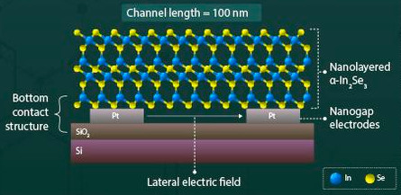
The bottom-contact transistor has been made by dropping a flake (~29nm thick) of α-In2Se3 onto contacts rather than growing the material from the bottom-up.
“When fabricating bottom-contact ferroelectric field-effect transistors by 2D material exfoliation, wide electrode width is preferred to improve the overall yield,” said Tokyo Tech. “However, achieving nanoscale channel lengths for the nanogap electrodes becomes challenging when simultaneously employing wide electrode widths, mainly due to the substantial ratio between the electrode width and channel length.”
The answer was a memory device with a two-terminal nano-gap-structured bottom contact (see diagram) that uses the in-plane polarisation flipping possible with α-In2Se3.
Flipping is initiated by applying a drain voltage via a channel with a “relatively narrow”, said Tokyo, length of 100nm – the distance between the inner edges of the platinum source and drain electrodes. The gate is the heavily-n-doped silicon substrate, which is insulated with a thin oxide layer.
This lateral structure is, in theory, compatible with conventional semiconductor device fabrication, said the university.
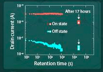
The proof-of-concept memory switches resistivity with a 103 on-off ratio, 17 hour data retention and 1,200 cycle endurance.
±5V on the gate was enough to polarise the ferroelectric, ±20V sweeping on the gate and +10V on the drain gave a drain current flow hysteresis loop with just under 10μA of difference between the 0Vg states.
“We believe that this design will pave the way in which data is stored and accessed and open up exciting opportunities for various applications, including artificial intelligence, edge computing, and Internet of Things devices,” said team leader by Professor Yutaka Majima.
Details of the research can be found in ‘Bottom contact 100 nm channel-length α-In2Se3 in-plane ferroelectric memory‘, published in Advanced Science. The paper is clearly written and can be read without payment.


