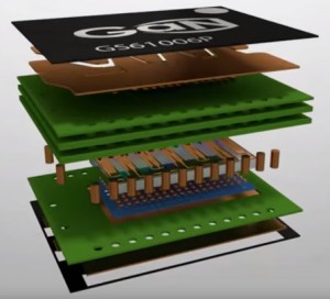
“Within a decade, we envision that America will both manufacture and package the world’s most sophisticated chips,” says Laurie Locascio director of the US National Institute of Standards and Technology (NIST), “this means both onshoring a high-volume advanced packaging industry that is self-sustaining, profitable and environmentally sound, and conducting the research to accelerate new packaging approaches to market.”
“The Vision for the National Advanced Packaging Manufacturing Program” (NAPMP), details the vision, mission and objectives for the advanced packaging program created by the Chips Act.
The intention is to deliver a “vibrant, self-sustaining, high, volume, domestic, advanced packaging industry, where advanced-node chips, manufactured in the US, are packaged in the US”.

The NAPMP will invest in design and simulation tools, manufacturing equipment and processes, R&D in materials and substrates, power delivery, and thermal management for advanced, packaging assemblies, a chiplet ecosystem, co-design of multi-chiplet subsystems with automated tools adapted for advanced packaging with consideration for built in test and repair, security, interoperability, and reliability.”
The Advanced Packaging Piloting Facility (APPF) will support the transitioning of these developments into high volume manufacturing.


