 The two companies confirmed tapeout of a multi-die test chip combining 3DFabric and UCIe PHY IP. They also announce routing capabilities for TSMC’s A16 process and EDA tools for mutual customers via TSMC’s Cloud Certification.
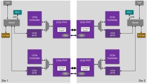
The tapeout of the test chip featuring a multi-die design using TSMC’s CoWoS packaging technology sets the stage, said Synopsys, for billion-to-trillion transistor designs in the future. The test chip combines TSMC’s 3DFabric technology and Synopsys’ tools for multi-die design, i.e., UCIe IP, 3DIC Compiler unified exploration-to-signoff platform, 3DSO.ai AI-enabled system analysis and optimisation, and silicon lifecycle management IP.
The 3DIC Compiler combines automated die-to-die routing and with signal integrity analysis while the UCIe PHY IP on TSMC’s advanced process and packaging technology exhibited robust die-to-die connectivity, reports Synopsys. Its Silicon Lifecycle Management & test IP for the UCIe PHY offers mission mode monitoring, testing, debugging, and repair during design, ramp-up, production, and field operation. IC Validator was used for physical verification of the multi-die design for design rule checking (DRC) and layout versus schematic (LVS) checking.
The partners also announced new routing capabilities to support TSMC’s A16 process in the digital design flow for power distribution and signal routing. This helps increase transistor performance efficiency and density.
Interoperable process design kits (iPDKs) and IC Validator physical verification runsets are available to handle the increasing complexity of physical verification rules and efficiently transition designs to TSMC N2 technology.
Finally, Synopsys EDA tools are enabled for mutual customers via the cloud through TSMC’s Cloud Certification to seamlessly integrate with TSMC’s process technology.