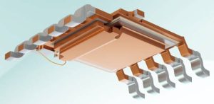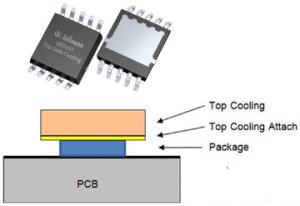
The package, SSO10T, has a 10μm gap instead of a thermal pad on the PCB side, and around 95% of heat will leave through the top, according to the company, typically to the ECU housing or a cold-plate.
It is expected to be used with a thermal interface pad to accommodate tolerance between PCB and heatsink surface.

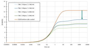
“SSO10T is based on the industry standard SSO8,” it said. “However, due to its top-side cooling, the SSO10 offers more than 20% and up to 50% higher performance than the standard SSO8 – depending on the thermal interface material used and the its thickness.”
As a thermal patch and thermal vias are no longer required on the PCB, the company predicts that some designs will be able to use simple double-sided PCBs.
So far, the company has released four mosfets in the package, all 40V n-channel:
- IAUCN04S6N007T 0.75mΩ 120A (390A) 100nC Qg
- IAUCN04S6N009T 0.90mΩ 120A (330A) 85nC Qg
- IAUCN04S6N013T 1.32mΩ 120A (230A) 52nC Qg
- IAUCN04S6N017T 1.73mΩ 120A (200A) 37nC Qg
All these figures are at 25°C. 120A is a nominal limit that is affected by external thermal design, while the die limit is in brackets. Higher pulses can be handled: for example …N007T can handle 1.3kA for 100μs.

Use is foreseen in brushless dc drives including electric power steering, dc-dc converters, safety switches and reverse battery protection.
The package has a JEDEC number allowing devices to be second-sourced.
Find some SSO10T information on this web page – the second video down is informative, and gets going properly at ~4mins.


