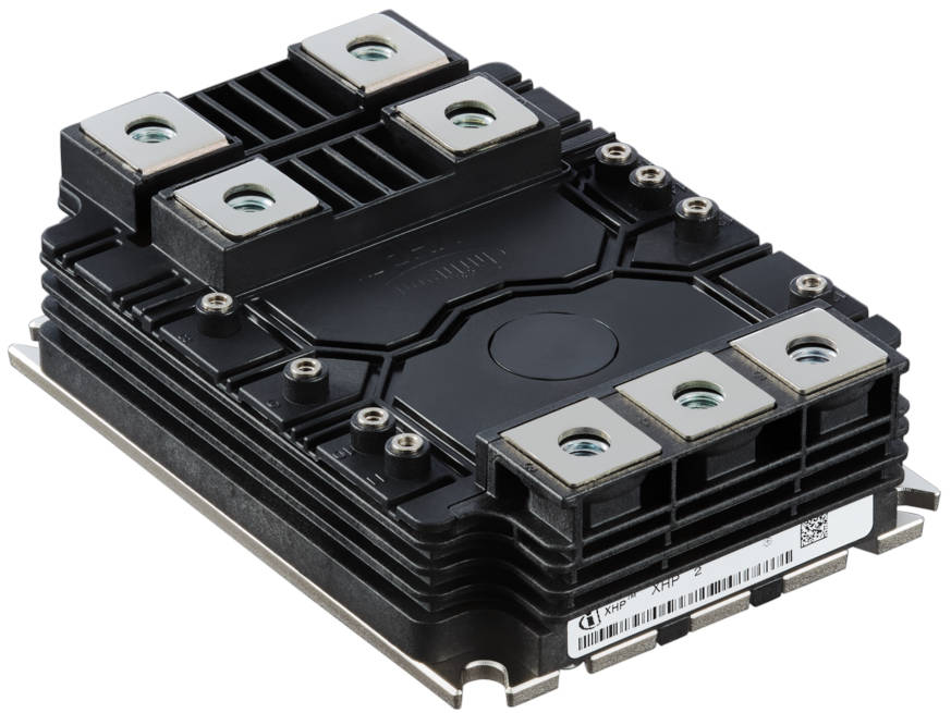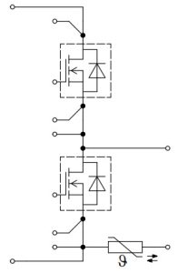
This package is rated for 6kV testing, and achieves 2.6kV partial discharge extinction. Creepage is 40mm terminal to baseplate and 34mm between terminals. Clearance is 31 and 8mm respectively.
The module’s mosfets, which can handle 2,000A repetitive pulses, expect 15 – 18V gate drive to turn them on and -5V to turn them off, and the gates can withstand -7 to +20V (-10 to +23V transients).
Total gate charge is 5µC (1.8kVdd, -5 to +15V).
Turn on and turn off times depend on multiple factors, and are typically around 450ns and 350ns respectively (1.8kV, 1kA). Rise and fall times are similarly variable, but around 200ns and 80ns.
The mosfet body diodes are similarly rated at 1,000A and drop a maximum of 4.9V at 125°C (3.9V typ). Recovery energy is typically under 100mJ.
The baseplate is made from aluminium silicon carbide, leading to a junction to case thermal resistance of 21.5°C/kW.
This week, this SiC die technology was short-listed for a German Federal President’s Award for Technology and Innovation (Deutscher Zukunftspreis 2024).
“A team of developers from Infineon, together with Chemnitz University of Technology, developed the world’s first silicon carbide mosfet with a vertical channel, and copper contacting, in the 3300V class,” said Infineon, explaining: Trench mosfets differ from so-called planar mosfets in their cell structure and performance. While the current flow in planar mosfets is initially horizontal, trench mosfets offer purely vertical channels. This results in a higher cell density per surface area, which in turn significantly reduces the losses in the chip during energy conversion.”
The nominated team is: Konrad Schraml (Infineon), Caspar Leendertz (Infineon) and Professor Thomas Basler (Chemnitz University of Technology) – results are out in November.
Find the 3.3kV FF2000UXTR33T2M1 on this web page


