They described the device at ISSCC in San Francisco this week.
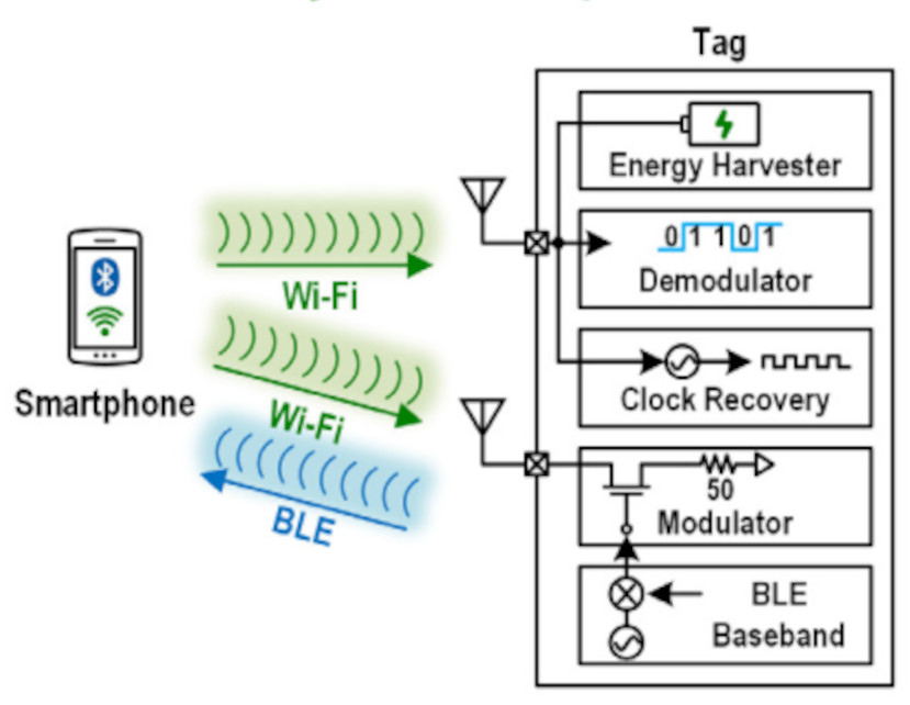
The tag has two antennas, with both used to extract power from the incident Wi-Fi field. One also receives the Wi-Fi (802.11b) signal for decoding and clock-recovery, while the other handles Bluetooth using frequency-division-duplex communication.
Bluetooth transmission energy is back-scattered from the Wi-Fi field by appropriately modulating a 50Ω load on the Bluetooth antenna – the required phase-compensation is demonstrated for the first time in this project, according to the team.
Internally, the received Wi-Fi signal is reprocessed using a novel ‘phase-flip’ tracking technique which both demodulates the DBPSK Wi-Fi signal, provides a clean CW carrier signal for Bluetooth signal generation, and recovers a 500kHz clock signal which, via an injection-locked ring oscillator, is made into a stable 8MHz system clock.
The IC was made on a 65nm cmos process and occupies 0.95mm2.
Both down-link and up-link operate at 1Mbit/s, and maximum system power is 17μW.
In the prototype, Wi-Fi Ch7 (2.442GHz) energy was used to sent out data on BLE Ch39 2.48GHz.
ISSCC24 paper 23.3 A passive crystal-less Wi-Fi-to-BLE tag demonstrating battery-free FDD communication with smartphones.


