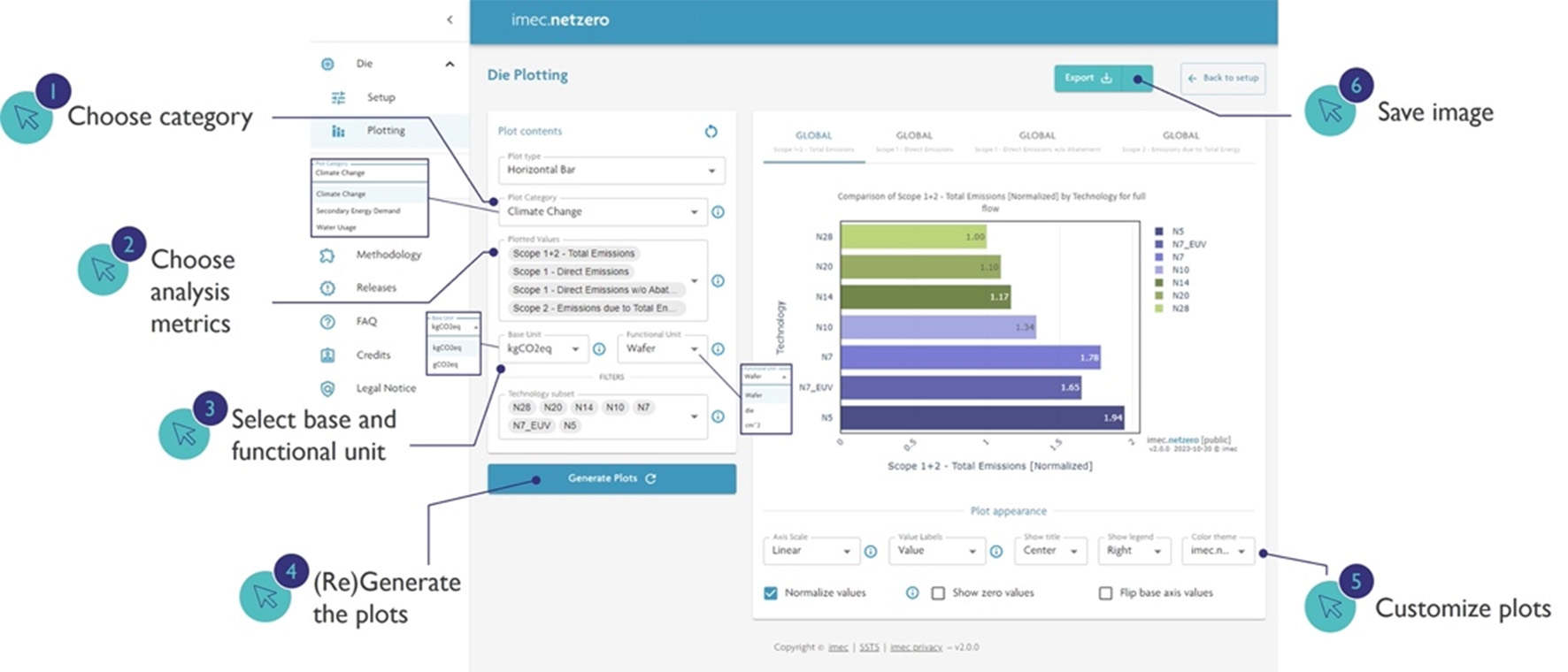
Called imec.netzero, it is built on an in-house virtual model of a fab and its supply chain.
“The tool provides valuable insights for academics, policy makers and designers,” according to Imec, which “aims to support industry in reducing its environmental impact, beyond the semiconductor supply chain”.
Data for the model comes from Imec’s own large-scale research fab in Leuven, and from the lab’s partner companies, including Samsung, TSMC, GlobalFoundries, ASML, Applied Materials, Tokyo Electron, Air Liquide, ASM, Edwards, Kurita, Lam Research and Screen.
Life-cycle assessment is used, based on an analysis of the energy, materials, chemicals, gases and other resources used in each process step of making an IC.
“Partners can access a private imec.netzero software application, that provides a detailed analysis to quantify embodied emissions and other environmental impacts about current and future IC technologies, providing tangible actions,” said Imec.
The public imec.netzero portal accesses the same fab models and process databases as the private portal, but can only display current technologies, and Scope 1+2 of the Greenhouse Gas Protocol.
It “provides unique insights into data otherwise not accessible to the public”, said Imec, “For example, visual presentations of CO2 emissions, electrical energy consumption or total water usage can be generated for multiple logic and memory technologies – from N28 onwards – based on fabrication in diverse geographical locations.”


