N-channel diamond mosfets have not proved so easy, blocking the route to diamond CMOS and all the high-voltage (bandgap = 5.5eV), high temperature and high thermal conductivity advantages that it might bring.
Now researchers at Japan’s National Institute for Materials Science (NIMS) have made n-channel diamond mosfets, by finding a way to phosphorus-dope the carbon lattice without: too much phosphorus, the large atoms doing too much damage, or the phosphorus atoms bringing dopant-neutralising hydrogen with them.
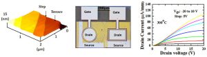
The result is a mosfet with ~150cm2/V/s field-effect mobility at 300°C – the graph shows curves from Vg = -20V (black line) to Vg = +10V (yellow).
The epitaxy was grown using microwave plasma chemical vapor deposition equipment made at the institute, which allowed over-doping to be avoided, and the resulting layers were atomically flat, with only a slight angle in the cut of the underlying substrate causing steps in the epitaxy surfaces.
Part of the key to the device is having a low-doped (≈1017/cm3 ) n-channel layer on the synthetic diamond substrate, over-laid by highly-doped epitaxy. “The use of the latter diamond layer significantly reduced source and drain contact resistance,” according to the Institute.
For more information, the Advanced Science paper ‘High-temperature and high-electron mobility metal-oxide-semiconductor field-effect transistors based on n-type diamond‘ can be read in full without payment.