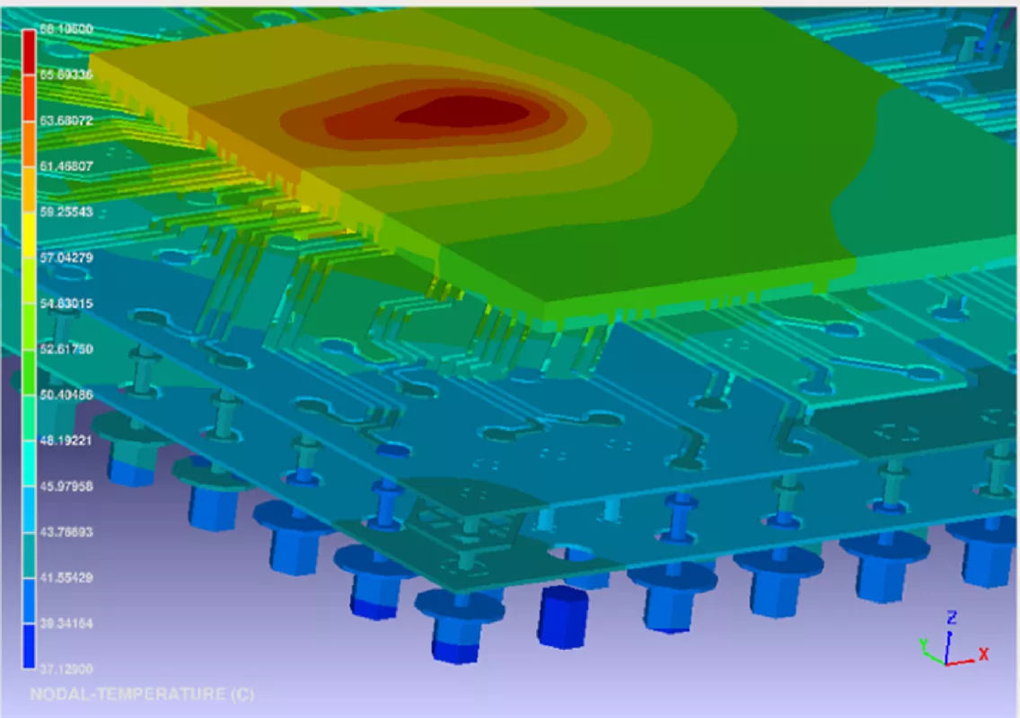
The 3.5D XDSiP integrates more than 6000 mm2 of silicon and up to 12 high bandwidth memory (HBM) stacks in one packaged device to enable high-efficiency, low-power computing for AI at scale. Broadcom says it has launched the industry’s first Face-to-Face (F2F) 3.5D XPU.
The computational power required for training generative AI models relies on massive clusters of 100,000 growing to 1 million XPUs. These XPUs demand increasingly sophisticated integration of compute, memory, and I/O capabilities to achieve the necessary performance while minimizing power consumption and cost.

Broadcom’s 3.5D XDSiP platform utilises F2F 3D-IC technology from TSMC to achieve significant improvements in interconnect density and power efficiency compared to traditional Face-to-Back (F2B) approach.
This F2F stacking employs hybrid copper bond (HCB) technology to directly connect the top metal layers of the top and bottom dies. HCB provides a dense and reliable connection with minimal electrical interference and exceptional mechanical strength.
Broadcom’s 3.5D platform includes IP & proprietary design flow for efficient correct-by- construction of 3D die stacking for power, clock and signal interconnects.
Benefits are:
- Enhanced Interconnect Density: Achieves a 7x increase in signal density between stacked dies compared to F2B technology.
- Superior Power Efficiency: Delivers a 10x reduction in power consumption in die-to-die interfaces by utilizing 3D HCB instead of planar die-to-die PHYs.
- Reduced Latency: Minimizes latency between compute, memory, and I/O components within the 3D stack.
- Compact Form Factor: Enables smaller interposer and package sizes, resulting in cost savings and improved package warpage.
Broadcom’s lead F2F 3.5D XPU integrates four compute dies, one I/O dies, and six HBM modules, leveraging TSMC’s cutting-edge process nodes, 3D die stacking, and 2.5D CoWoS packaging technologies.
The 3.5D XDSiP has, says Broadcom, demonstrated complete functionality across critical IP blocks, including high-speed SerDes, HBM memory interfaces, and die-to-die interconnects.


