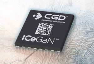
“Although we have a great deal of data to prove the ruggedness and reliability of our hemts, GaN is still a relatively new technology, certainly when compared to traditional silicon for power electronics applications,” said company CEO Giorgia Longobardi. “By incorporating 2D barcodes we are able to provide feedback to our manufacturing supply chain, which helps cement our relationships and scale-up for high volume manufacture.”
“We know, for example, that yields are lowest at the wafer edge,” said v-p of operations Zahid Ansari. “Now we can see how the position on the wafer might affect device performance. This information can be fed back to the foundry to enable continuous manufacturing process improvements.”
The companies GaN power devices are ICs, with components alongside the main hemt to improve gate characteristics and add other functions – for example, some can be driven with conventional gate drivers made for silicon mosfets, rather than needing special GaN gate drivers.
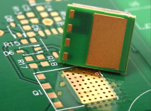
To lower hurdles to adopting its GaN devices, CGD recently announced a series of adaptor boards (left) that make its 5×6 and 8×8 DFN packaged transistors into drop-in replacements for other devices from other manufactures: GaN hemts and silicon mosfets from GaN Systems, Infineon, Innoscience, Navitas and Transform, plus generics for TO-220 and TO-247 devices.
CGD is a 2016 from the University of Cambridge with private seed, series A and series B funding.
CGD interface board list