
“Over the past decade, the consecutive introduction of 100G, 200G and 400G pluggable optics has enabled cloud datacenters to support the ever-growing demand for a plethora of applications, such as video streaming, web browsing, social networking, cloud computing and many more,” says Van Campenhout, “continuing this evolution, 800G pluggable modules will soon enter the field and 1.6T optics are expected by 2026, interconnecting the datacenter switches through single-mode fiber cabling across hundred meters of distance.”
“The continued bandwidth increase in datacenter networking is on the one hand driven by the CMOS scaling of the datacenter switches, and on the other hand by the evolving IEEE Ethernet transceiver (TxRx) standards,” he continues, “historically, the lowest cost transceiver solutions have been obtained by minimizing the number of parallel optical channels or lanes. Therefore, the key scaling vector is the baud rate (or signaling rate) of the optical transceiver, which refers to the number of symbols that can be transmitted per second through a single optical channel. The first generation of 1.6T pluggable optics will be implemented with eight parallel lanes, each carrying 200 gigabits per second (Gbps), by scaling baud rates to 100 gigabaud (Gbd) combined with four-level pulse-amplitude modulation (PAM-4). For the subsequent generation running at 400Gbps per lane, baud rates will likely scale to 140Gbd and modulation formats will grow even more complex.”
“The key scaling vector is the baud rate (or signaling rate) of the optical transceiver, which refers to the number of symbols that can be transmitted per second through a single optical channel,” says Van Campenhout, “the evolution towards higher baud rates drives the development of high-bandwidth electro-optical modulators and photodetectors. Insufficient bandwidth of the electro-optical channels results in degraded data transmission quality. This needs to be mitigated with advanced digital signal processing (DSP), implemented in the most advanced CMOS nodes. But DSP adds considerable power, latency and cost. Therefore, there is a clear demand for optical components with bandwidths beyond 100GHz that would substantially reduce the need for DSP.”
“Over the past years, imec has advanced the state-of-the-art in Si photonics (SiPho) technology as part of the Optical I/O program. Many Si- and Ge-based electro-optical components have been demonstrated at 50GHz bandwidth, enabling 200Gbps PAM-4 transmission for the upcoming, first-generation 1.6T pluggable optics,” says Van Campenhou, “recently, we also realized the integration of high-quality low-pressure chemical vapor deposition (LPCVD)-based SiN waveguides in our SiPho platform, complementing our toolbox with high-precision passive optical components. Moreover, we developed the SiPho interfaces for flip-chip-based III-V laser integration, which will help to reduce overall transceiver cost. Using this process, we recently demonstrated indium-phosphide (InP) distributed-feedback (DFB) laser diodes bonded onto silicon photonics wafers with an alignment precision within 300nm and coupling loss less than 2dB.”
“For lane rates at 400Gbps, the SiPho toolbox needs a major upgrade,” he continues’ “Especially on the transmission side, modulators with bandwidth beyond 100GHz and sufficiently low optical losses are very hard to achieve in Si or Ge, which necessitates the introduction of “exotic” electro-optic materials such as LiNbO3, BaTiO3 or chromophore polymers. We are carrying out early integration pathfinding efforts aimed at the hybrid or heterogeneous integration of such non-CMOS materials in the SiPho process flow, e.g., exploring techniques such as microtransfer printing. In addition, IDLab, an imec research group at Ghent University, has recently demonstrated SiGe BiCMOS analog front-end electronics capable of driving the SiPho modulators and photodetectors at 200Gbps/lane.”
“The recent arrival of large, generative AI models such as ChatGPT, GPT-4 and Lambda has put a spotlight on the importance of sufficient networking bandwidth for high-performance AI/ML clusters, used for training such models,” adds says Van Campenhout, “pluggable optical interconnects have already started to replace Cu interconnects within such compute clusters, interconnecting the multi-XPU servers across distances of a few to tens of meters. As these clusters scale to thousands of XPUs, optical interconnects will gradually move into the board and package, to meet the high chip-to-chip interconnect bandwidth requirements. This evolution puts even more pressure on metrics like bandwidth density, cost, power, and reliability. Optical transceivers with multi-Tbps/mm bandwidth density, power consumption well below 5pJ/bit, low link latency (<100ns), and high reliability will be needed – all at a cost of 10c$/Gbps or less.”
”As AI/ML clusters will scale to thousands of XPUs, optical interconnects will gradually move into the board and package, to meet the high chip-to-chip interconnect bandwidth requirements,” says says Van Campenhout.
“Unlike for datacenter networks, the tight power and latency budgets leave no or very little room for digital signal processing,” he continues, “this means that the optical channels need to be very ‘clean’, with extremely low bit error rates. Therefore, for these systems, a more appropriate way to scale bandwidth is by using a larger number of parallel optical channels, each running error-free at modest data rates in the range of 16-64Gbps, using optical and electrical components optimized for efficiency rather than bandwidth. Aggressive wavelength division multiplexing (WDM) with 8, 16 or more wavelengths in turn helps to keep the total number of physical optical channels in check. To connect the optical I/O modules with the XPU or high bandwidth memory (HBM) stacks, wafer-level co-packaged optics is emerging, leveraging the power-efficient electrical wide-I/O electrical interfaces for the “last-mile” copper interconnects. Finally, cost and optical link budgets are increasingly driving for integration of the light sources onto the SiPho chips.”
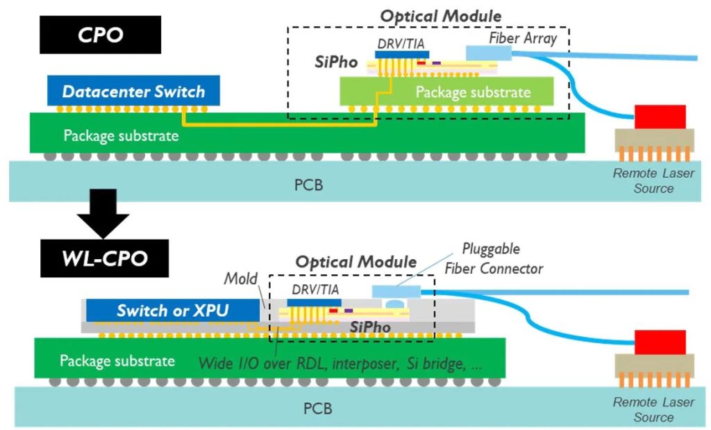 Imec’s vision for wafer-level CPO (WL-CPO), with aggressive WDM scaling.
“For both cloud datacenters and AI/ML clusters, networking bandwidth has become an increasingly important metric determining system-level performance,” continues says Van Campenhout, “the networking bottleneck has created a high sense of urgency, translating into strong engagements for silicon photonics adoption by the industry.
“Recent research activities focus, among others, on optimizing silicon ring modulators, WDM filters and circuits for enabling low-power hybrid CMOS-SiPho transceivers. Ring-based WDM SiPho transceiver architectures show great potential to realize the performance metrics required for AI/ML cluster applications. At the 2023 Optical Networking and Communication Conference (OFC 2023), imec demonstrated an “error-free” (i.e., bit error rate <10-12) ring-based CMOS-SiPho transceiver with optical energy consumption as low as 3.5pJ/bit. The solution is scalable to 800Gbps/mm bandwidth density, using 8 wavelengths.”
”The move towards SiPho transceivers with a growing number of optical lanes comes with a higher risk of yield loss,” he adds, “this should be avoided as much as possible from a cost perspective. Therefore, to measure and subsequently improve yield, we are developing wafer-scale solutions for known-good die (KGD) testing of the SiPho transceivers.”
“Wafer-level co-packaged optics combined with aggressive WDM is considered a viable approach towards 2-4Tbps/mm fiber-coupled optical links for AI/ML system applications, with power consumption down to 1-2pJ/bit,” continues says Van Campenhout, “but, by the end of the decade, we anticipate the need for optical interconnects approaching 10Tbps/mm bandwidth density, at power consumption well below 1pJ/bit. We recently started pathfinding activities towards wafer-level optical interconnects, our long-term vision for ultrahigh-bandwidth chip-to-chip optical I/O. This deeply integrated optical I/O technology will ultimately enable massively parallel, optical XPU-to-XPU connectivity, promising tremendous gains in system performance.”
“By the end of the decade, we anticipate the need for optical interconnects approaching 10Tbps/mm bandwidth density, at power consumption well below 1pJ/bit,” he says m.
“Since the start of the Optical I/O program in 2010, imec has acquired a wealth of know-how in developing silicon integrated photonics, thereby leveraging decades of CMOS integration knowledge. Furthermore, advanced implementations of co-packaged optics require cutting-edge 3D integration technologies, for which we can rely on the years of experience gained within imec’s 3D system integration program. In the same realm, our long-term vision to introduce optical interconnects in the wafer-level package needs to be supported by a system-level analysis, for which we are collaborating with imec’s system-technology co-optimization (STCO) team. The unique availability of such diverse competences under one roof, together with the strong presence of our partner ecosystem, fosters the exchange of ideas and accelerates the development of highly complex systems and technologies.”
“Conversely, developments in the context of the optical I/O program feed other application-oriented integrated photonics activities pursued within imec – such as next-gen LiDAR, quantum cryptography, consumer health, medical diagnostics and agrifood – some of them in collaboration with partners from the Dutch PhotonDelta ecosystem, ” concludes Van Campenhout.


