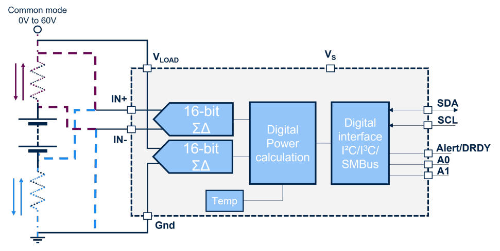
Called TSC1641, it has two 16bit ΣΔ converters at its inputs, allowing simultaneous measurement of current (LSB=2.5µV) and voltage (LSB=2mV).
The measured voltage can be anywhere from 0 to 60V (65V abs max), and the two current terminals sense with either polarity across a sense resistor anywhere in that voltage range – so high-side or low-side current sensing is possible, bidirectional in both cases.
Shunt sensing amplitude is between -81.9175 and +81.92mV, with a typical offset voltage of ±3µV. Both voltage and current measurements have a maximum gain error of 0.5%.
Input bias current is typically 20pA with a common-mode voltage of 12V.
Control is over a choice of 1MHz I2C/SMbus or 12.5MHz I3C, and parameters that can be set across this include assertion levels of alerts for voltage (under/over), current (under/over), power (over) and temperature (over) – it is SMBus alert compatible.
A separate supply between 2.7 and 3.6V is needed to power the chip, at up to 1.4mA, but typically 1mA – this is dependent on the conversion time, which can be programmed between 128µs and 32.7ms. The device can also be shut-down, typically to 50nA.
Operation is over -40 to +125°C, and the package is a 3 x 3mm plastic DFN10.
STEVAL-DIGAFEV1 is the matching evaluation board, which can be controlled from the STM32 MCU based NUCLEO-H503RB development board, for which STSW-DIGAFEV1GUI is a graphical user interface to configure the new IC, and STSW-DIGAFEV1FW is sample firmware for it.
“TSC1641 helps optimise energy use and reliability in industrial battery packs, power inverters, dc power supplies, data-center and telecom equipment and power tools,” said ST.
Find the TSC1641 product page here


